Researchers in Switzerland have fabricated perovskite-silicon tandem solar cells that use a heterojunction cell as the bottom device. The cell is said to circumvent the film formation problem associated with the use of phosphonic acid and achieve high levels of efficiency.
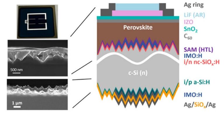
Scientists from the École Polytechnique Fédérale de Lausanne (EPFL) in Switzerland have fabricated a tandem solar cell based on a perovskite top cell and a heterojunction (HJT) bottom device with a thickness of 100-150 μm and double-sided microstructured surfaces.
“The concept of double-sided textured bottom cells is a major design adjustment of current champion devices, such as those from King Abdullah University of Science and Technology (KAUST), which achieve an energy conversion efficiency of 33.7%, and Longi, which holds the world record with an excellent efficiency of 33.9% and recently 34.6% on Cz-silicon (Cz-Si) bottom cells,” they stated.
The research team explained that the HJT cell was fabricated by wet-etching random pyramids, adjusting their height by alkaline texturing without power loss in the cell.
“To realize high-performance shunt-free perovskite/silicon tandem solar cells with solution-processed top cells with high efficiency, the thickness of the perovskite absorber must be thicker than the height of the pyramid texture,” the report points out. “Since high-performance wide bandgap perovskite absorbers are typically 600-800 nm thick and usually do not conformally cover the surface when processed from solution, the height of the pyramid must be adjusted accordingly.”
The scientists built the top cell with a hole transport layer (HTL) with a self-assembled monolayer (SAM) based on [2-(3,6-Dimethoxy-9H-carbazol-9-yl)ethyl]phosphonic acid (MeO-2PACz), a perovskite absorber, an electron transport layer (ETL) made of tin oxide (SnO2) And buckminsterfullerene (C60), a transparent back contact made of indium zinc oxide (IZO), and a silver (Ag) metal contact.
The bottom cell was fabricated with a-Si:H(i)/nc-SiOx:H(N) layer stack on the front and an a-Si:H(i)/a-Si:H(p) layer stack on the back, deposited using plasma-enhanced chemical vapor deposition (PECVD). “A layer stack of transparent conducting oxide was sputtered by DC sputtering at the back and 20 nm at the front, defining the cell surface of approximately 1 cm.2 by aligned sputter masks on both sides.
Tested under standard lighting conditions, the tandem cell achieved an efficiency of 30.22%, an open-circuit voltage of 1.954 V, a short-circuit current density of 18.92 mA/cm2 and a fill factor of 81.74%.
“These results demonstrate the potential of submicron-sized textured Cz silicon bottom cells for industry-compatible tandem cells with solution-processed perovskite top cells to achieve high efficiency,” the scientists noted. “Additionally, our work demonstrates a simple, implementable solution to circumvent the film formation problem associated with Me-4PACz while maintaining a high charge extraction rate and good passivation properties.”
The new cell concept was described in “Perovskite/silicon tandem solar cells More than 30% conversion efficiency on submicron structured Czochralski silicon bottom cells with improved hole transport layers”, published in ACS applied materials and interfaces.
This content is copyrighted and may not be reused. If you would like to collaborate with us and reuse some of our content, please contact: editors@pv-magazine.com.


