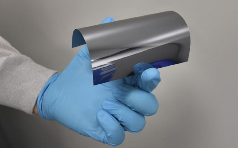
The German wafer manufacturer said the efficiency was achieved using an unspecified commercial M6 HJT production line, without specifying whether the result had been certified by an independent third party.
German wafer manufacturer NexWafe GmbH has announced that it has achieved an energy conversion efficiency of 24.4% for a heterojunction (HJT) solar cell built with its ultra-thin wafers.
The company said the efficiencies were achieved using an unspecified commercial M6 HJT production line, without specifying whether the results had been certified by an independent third party.
“The result confirms that NexWafe’s direct gas-to-wafer process is a complete replacement for conventional Czochralski (CZ) wafers, while offering the potential for significant cost savings by reducing material losses and energy consumption by 40% and eliminating the saw damage etching step cell production,” it added. “The oxygen content of EpiNex wafers is also 20 times lower than that of conventional CZ wafers. This enables thermal stability and helps improve cell performance.”
The company also said it has developed a perovskite-silicon tandem solar cell in collaboration with the Swiss Center for Electronics and Microtechnology (CSEM) achieved an energy conversion efficiency of 28.9%.
The manufacturer claims its EpiWafers technology could help module makers achieve dramatically higher yields without having to upgrade their production lines. It also claims that its technology can enable the production of ultra-thin wafers. It has already demonstrated this on its pilot line in Freiburg, Germany.
NexWafe develops and produces monocrystalline silicon wafers grown directly from cheap raw materials. The continuous, direct gas-to-wafer manufacturing process eliminates the need for costly and energy-intensive intermediate steps, such as polysilicon production and billet drawing, that traditional wafer manufacturing relies on. The process also reportedly minimizes waste, reducing wafer production costs by as much as 30%. According to the company, it also reduces carbon dioxide emissions by 70% during production.
NexWafe plans to commission its epitaxial facility in Bitterfeld, Anhalt-Bitterfeld district, Saxony-Anhalt, Germany, by June 2025.
“This innovative system uses advanced heating systems and chemical vapor deposition at atmospheric pressure to deposit monocrystalline silicon over an area of 1.3 m x 50 cm, equivalent to more than fourteen G12 wafers at once,” it explains. “With proven deposition rates of 5 microns per minute and temperature uniformity that achieves a total thickness variation (TTV) of less than 40%, this platform represents a significant leap in production scalability.”
This content is copyrighted and may not be reused. If you would like to collaborate with us and reuse some of our content, please contact: editors@pv-magazine.com.


