In a new paper published in Nature Communications, the Chinese solar manufacturer explained that the heterojunction back contact cell it unveiled in late 2023 achieved one of the highest open-circuit voltages ever reported for this cell technology, as well as a smaller-than-usual short-circuit voltage . current losses. The results were confirmed by the German Institute for Solar Energy Research (ISFH).
A group of scientists from Chinese solar module manufacturer Longi has described in a new scientific paper the 27.09% efficient heterojunction back contact (HBC) solar cell it unveiled in December 2023.
At the time, Longi said only that the result was made possible by a new laser graphics process that costs less than conventional, expensive photolithography processes, without providing further details. In the new paperthe company explained that the laser pattern technology had been developed by Longi itself. Furthermore, it not only provided a thorough technical description of the cell architecture, but also presented a strategy for improving contact resistance, series resistance, and backside pattern design.
The group specified that HBC solar cells have problems with carrier recombination losses and said these arise from the hole-selective contact area and polarity boundaries. “We propose solutions to these problems and establish a clear relationship between contact resistance, series resistance and the design of the backside pattern,” she added.
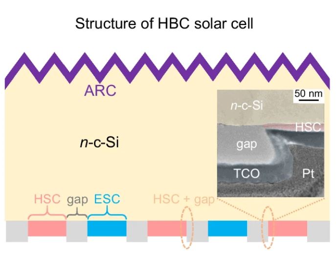
The research group built the 243.0 cm2 cell with a 200 µm thick Longi M6 274.3 cm2 Czochralski wafer based on n-type monocrystalline silicon. The front features anti-reflective coatings (ARC) and the back is divided into four areas: hole-selective contact (HSC), gap area, electron-selective contact (ESC), and HSC plus gap.
“We have exploited amorphous silicon as passivating contact layers and laser ablation as mass production technology for manufacturing HBC solar cells,” the academics explained. “This provides advantages including low leakage in the region near the np polarity boundary, low cost, low deposition difficulty and high uniformity.”
Using laser patterning, the researchers applied a pulsed green picosecond laser to ablate the overlying ia-Si:H/pa-Si:H stack in the designed ESC region. The transparent conductive oxide layer (TCO) was deposited using the magnetron sputtering technique.
They also used a pulsed ultraviolet picosecond laser to ablate the designed gap region to remove the TCO/pa-Si:H/ia-Si:H stack for isolation, which they say avoids leakage channels. The silicon nitride (SiNX) layer was used to avoid damaging the passivation performance of the ia-Si:H/na-Si:H stack.
Tested under standard lighting conditions, the device achieved an energy conversion efficiency of 27.07% and an open-circuit voltage of 751 mV, with the results confirmed by the German Institute for Solar Energy Research (ISFH). The no-load voltage value is indicated by Longi as one of the highest ever recorded at research level for this type of solar cell.
Their analysis also revealed that the cell, like other HBC devices, suffers from electrical shadowing effects due to carriers for both polarities being collected on the same side, and the resulting decrease in short-circuit current density. However, they also found that these losses are slightly smaller than those seen in previous devices.
“This is mainly attributed to the additional current gain of the thicker silicon wafer and the designated illumination area used in measurements, which excludes the influences of recombination and leakage at the edge of the silicon wafer,” they further explained.
The group also found that contact resistance plays a crucial role in high-efficiency HBC solar cells and said that minimizing the contact area of the HSC or ESC region was crucial for improving cell efficiency. “By optimizing the HSC area, we achieved the lowest contact resistance using pa-Si:H film,” it specified. “Additionally, we found that the contribution of contact resistance to drag can be directly calculated from the coverage area ratio.”
Looking ahead, the researchers said they want to utilize wafer edge effects and implement “meticulous” optimization of the front anti-reflective coating and rear reflector, which they believe could help the cell achieve efficiency of up to 27.7%.
The solar cell architecture was described in “27.09%-efficiency silicon heterojunction back contact solar cell and going beyond,” published in communication about nature. “The research provides multiple strategies and guidelines for optimizing structural design and resolving major contradictions within back-contact solar cells,” the group pointed out.
This content is copyrighted and may not be reused. If you would like to collaborate with us and reuse some of our content, please contact: editors@pv-magazine.com.


