Scientists in Japan developed a 4.49% efficient solar cell based on titanium dioxide and selenium. The devices are based on a novel approach aimed at reducing interfacial recombination and increasing open-circuit voltage and efficiency.
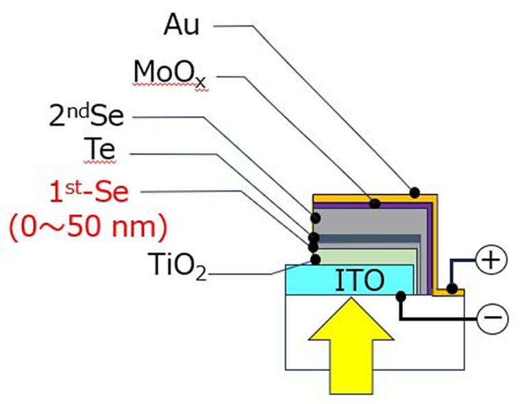
Researchers from Ritsumeikan University in Japan have fabricated a heterojunction solar cell that uses a window layer made of titanium oxide (TiO2) and a selenium (Se)-based absorber. The new device is based on a new architecture that reportedly increases the typical “insufficient” shunt resistance that characterizes these PV cells.
“We have developed an innovative approach to form crystallized Se (c-Se) using a stacked precursor based on Se and Tellurium (Te), with precise control of the interfacial Te content,” said the corresponding author of the research, Taizo Kobayashi, pv magazine. “The goal is to increase the adhesion between the TiO2 and Se layers, while limiting the deleterious effects of Te enrichment in terms of carrier transport, resulting in a significant improvement in the energy conversion efficiency of TiO2/Se heterojunction photovoltaic devices.”
The scientists explained that the key to their performance was minimizing areas of low resistance near the p-n junction caused by Te buildup, which increases interfacial recombination and is detrimental to the open-circuit voltage and overall efficiency of the cell . They used ‘commonly used’ equipment to apply a resistance heating evaporation technique in the production process.
“This advance provides a practical solution to overcome the difficulties associated with forming a uniform Te adhesion layer, making it accessible and applicable to a wider range of research groups,” they further explained.
The group built the solar cell with a substrate of glass and indium tin oxide (ITO), a buffer layer of zinc magnesium oxide (ZnMgO), the TiO2 window layer, a Se absorber, a buffer layer made of molybdenum trioxide (MoO3) and a gold (Au) metal contact.
“A 5 nm 1st-Se layer appears to be the sweet spot that allows a higher degree of control over the Te interface while limiting its deleterious impact on carrier transfer,” the team further explained. ”
Tested under standard lighting conditions, the solar cell achieved an energy conversion efficiency of 4.49%, an open circuit voltage of 0.795 V, a short circuit density of 11.13 mA/cm2 and a fill factor of 50.7%. The devices showed higher open-circuit voltage and lower dark leakage current values compared to similar devices developed in previous scientific work.
“Especially when the thickness of the 1st-Se layer was 5 nm, significant improvements in open-circuit voltage and efficiency were achieved compared to devices fabricated using a conventional process,” the academics pointed out. “The introduction of a 5 nm thick 1st-Se layer into 1st-Se/Te/2nd-Se played a crucial role in promoting the orientation and precisely controlling the Te/(Te + Se) ratio for efficient TiO2/Se photovoltaic devices close to the state of the art.”
They introduced the new cell technology in the study “TiO2/Se heterojunction photovoltaic device made from a stacked Se/Te/Se precursor”, published in Solar energy materials and solar cells.
This content is copyrighted and may not be reused. If you would like to collaborate with us and reuse some of our content, please contact: editors@pv-magazine.com.


