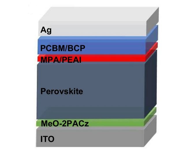
The inverse perovskite device, developed by researchers in China, reportedly achieves the smallest non-radiative recombination-induced open-circuit voltage drop reported to date. It uses a synergistic bimolecular interlayer to functionalize the perovskite interface.
A group of scientists led by Fudan University in China have developed an inverted perovskite solar cell that uses a synergistic bimolecular interlayer (SBI) and reportedly achieves the smallest non-radiative recombination-induced open-circuit voltage drop reported to date
Inverted perovskite cells have a device structure known as “pin”, where hole-selective contact p is at the bottom of the intrinsic perovskite layer i with electron transport layer n at the top. Conventional halide perovskite cells have the same structure, but in reverse: a ‘nip’ arrangement. With nip architecture, the solar cell is illuminated via the electron transport layer (ETL) side; in the pin structure, it is illuminated by the surface of the hole transport layer (HTL).
The researchers’ SBI strategy involved depositing 4-methoxyphenylphosphonic acid (MPA) and 2-phenylethylammonium iodide (PEAI) as modulators to functionalize the perovskite surface.
“MPA induces an in-situ chemical reaction on the perovskite surface via the formation of strong covalent PO-Pb bonds that reduce the density of surface defects and increase the Fermi level on the surface,” they explained. “PEAI further creates an additional negative surface dipole so that a more n-type perovskite surface is constructed, which improves electron extraction at the upper interface.”
They also emphasized that the proposed strategy does not affect perovskite surface morphology, crystallinity or optical absorption properties, while contributing to more effective passivation of defects.
The scientists built the cell with a substrate made of fluorine-doped tin oxide (FTO), called a hole transport layer (HTL) made of phosphonic acid methyl substmodified carbazole (Me-4PACz)a perovskite absorber, the SBI layer, a buckminsterfullerene (C60) electron transport layer (ETL) based on phenyl-C61-butyric acid methyl ester (PCBM), a bathocuproin (BCP) buffer layer and a silver (Ag) metal contact.
Using ultraviolet photoelectron spectroscopy (UPS), the team also found that the perovskite surface can pin onto the negative polaron transport state of PCBM ETL, further promoting electron transfer across the perovskite/ETL interface.
“In addition, the SBI-modified perovskite film exhibits smaller difference in surface potential distribution and lower surface roughness,” the team said. “A smoother perovskite surface with a more uniform surface potential distribution is beneficial for forming an efficient contact with the adjacent ETL that prevents non-radiative recombination.”
Popular content
Tested under standard lighting conditions, the solar cell achieved an efficiency of up to 25.53% and a short-circuit current density of 24.31 mA cm2. It also achieved one of the smallest non-radiative recombination-induced open-circuit voltage drops of “only 59 mV” and a certified efficiency of 25.05%. “In addition, the target device also exhibits good stability, retaining 95% of its initial efficiency for aging for more than 1,000 hours,” the academics added.
They described the new cell concept in the study “Reducing Non-radiative Recombination for High-Efficiency Inverted Perovskite Solar Cells via a Synergistic Bimolecular Interface”, which was recently published in communication about nature. “These results well demonstrate the important role of our SBI strategy on the properties of perovskite surfaces, showing significant effectiveness in minimizing trap density and constructing favorable perovskite surface energies, and paving ways for the further improvement of perovskite solar cells “, the scientists concluded.
This content is copyrighted and may not be reused. If you would like to collaborate with us and reuse some of our content, please contact: editors@pv-magazine.com.


