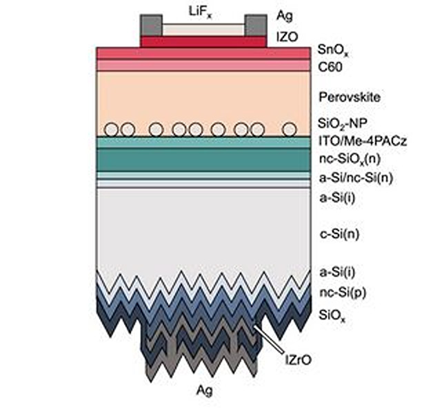
The tandem solar cell is based on a perovskite top cell treated with an additive known as 2,3,4,5,6-pentafluorobenzylphosphonic acid (pFBPA), which is said to improve energy conversion efficiency and fill factor. The tandem device also integrates a bottom-end heterojunction silicon cell made with a 190 μm thick, 2 Ω.cm, n-type, float-zone, gloss-etched monocrystalline wafer.
An international group of scientists led by the Ecole Polytechnique Federale de Lausanne (EPFL) in Switzerland has developed a perovskite-silicon tandem solar cell that integrates a top perovskite cell based on an absorber treated with 2,3,4,5,6-pentafluorobenzylphosphonic acid (pFBPA).
In the study “Synergistic substrate and additive engineering for more than 30% efficient perovskite-Si tandem solar cells,” published in Joulesaid the researchers that the use of pFBPA is intended to reduce lead-related defects in the perovskite film and non-radiative recombination near the perovskite absorber and electron transport layer, thereby increasing cell efficiency and filling factor.
The researchers also explained that the proposed cell configuration and associated manufacturing process eliminate the need for a post-deposition passivation treatment or an additional passivation layer, because the pFBPA was added to the perovskite precursor ink.
The team built the top cell with a substrate made of indium tin oxide (ITO), called a hole transport layer (HTL) that relies on silicon dioxide (SiO2) nanoparticles and phosphonic acid methyl substmodified carbazole (Me-4PACz)a perovskite absorber, an ETL based on buckminsterfullerene (C60), a buffer layer of silicon oxide (SiO2) nanoparticles (NPs), a transparent contact based on indium zinc oxide (IZO) and a silver (Ag) metal contact.
“As with PERC cells, the configuration consists of the insulating perovskite/SiO2-NP interface with high passivation quality and the HTL/perovskite interface through which the current passes and with a passivation quality worse than that achieved with the SiO2-NPs,” the academics explained. “Overall, the results show that caution is required when optimizing the SiO2-NP concentration, which is influenced by the choice of both HTL and perovskite composition, both of which can influence charge transport at the HTL/perovskite interface.”
The perovskite cell was integrated into a bottom cell tandem cell based on heterojunction (HJT) technology and fabricated with a 190 μm thick, 2 Ω.cm, n-type, float-zone, gloss-etched monocrystalline wafer. “The inverted structure, with the P-type contact at the bottom and Ntype at the top, is common to most high-efficiency perovskite-Si devices today due to the relatively transparent electron transport layers of the perovskite cell and the well-established SHJ technology that requires little modification to be integrated into tandems,” the group points out.
Tested under standard lighting conditions, the tandem device achieved an energy conversion efficiency of 30.9%. The scientists said the result was certified by an unspecified third party. They attributed the cell’s remarkable performance to the gains it could achieve pFBPAespecially when used in combination with a SiO2-NP-coated substrate, which they say in turn prevents the formation of holes and shunts resulting from the use of pFBPA.
“The wettability-enhancing SiO2-NPs also enable the reliable use of high-performance Me-4PACz as an HTL that further reduces shunt resistance (RS) and in particular improves the filling factor of the devices,” they concluded.
This content is copyrighted and may not be reused. If you would like to collaborate with us and reuse some of our content, please contact: editors@pv-magazine.com.


