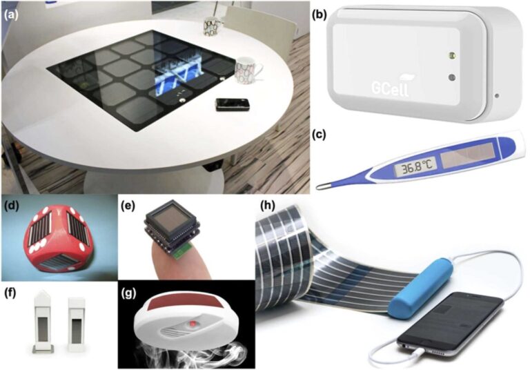
A review of indoor PV cell technologies by an international research team documents more than 250 commercial and laboratory devices for large and small areas. It includes organic, dye-sensitized and perovskite devices, as well as crystalline and amorphous silicon, III-V semiconductors, chalcogenide and emerging lead-free alternative cells.
“We noticed that interest in this field was really on the rise, so we believed that a comprehensive evaluation of all indoor PV technologies was needed,” said review co-author Giulia Lucarelli. pv magazine.
The review also includes a discussion of applications, recent advances, and strategies used to design more stable, highly efficient cells that operate at very low light levels.
“We provided the performance data of the indoor PV devices at 200 lx and 1000 lx illuminance,” said corresponding author Thomas M. Brown. pv magazineexplaining that most homes have an illuminance of 200 lx, while 1000 lx is typical in very well-lit environments such as supermarkets.
Brown pointed out that one of the initial high-volume market niches for indoor PV was electronic shelf labels in supermarkets. Other applications are emerging, such as Internet-of-Things products, where PV is seen as a ‘fit and forget’ approach, where a product is installed once with no further maintenance required. “Think about putting a temperature or other type of sensor in your home and letting it work there without ever having to replace the batteries,” says Brown.
The cell technologies covered in the review range from crystalline and amorphous silicon to III-V semiconductor and chalcogenide devices, as well as organic, dye-sensitized, perovskite and lead-free alternative devices.
Looking at energy conversion efficiency (PCE) and maximum power density (MPD), the team made several observations. For example, it was said that it was “clear that, regardless of indoor lamp type or intensity,” perovskite solar cells have “outpaced” other PV technologies in both efficiency and power output.
The team found that organic photovoltaic devices (OPV) performed well under light-emitting diodes (LED), while dye-sensitized solar cells (DSSC) performed better under fluorescent light (FL). But it also warned that there were only a limited number of reports, making it “difficult” to draw conclusions.
“Among the established technologies, compound and thin-film semiconductors have shown significant performance improvement in recent years, with the former delivering high efficiency and power output,” the team pointed out. “The lead-free alternatives have just entered the indoor PV arena and have managed to deliver the highest efficiency of around 18% with a tin-based perovskite.”
Standards for performance reporting were discussed, in particular the need for a protocol for measurements in the standard light source spectrum and a standard illumination level(s). “The most commonly used currently are 200 lx and 1000 lx, so both should remain reported,” the scientists said.
They explained that MPD reporting for illuminances of 200 lx and 1000 lx is important for product developers designing energy harvesting solutions and products that operate in a range of lighting conditions. “MPD is a more direct measure, because product developers who want to integrate PV into their products know exactly what comes out of the PV device,” said co-author Abhisek Chakraborty. pv magazine.
Brown added that the spectra of indoor lamps are diverse, ranging from LED to compact fluorescent lamps and lamps with different color temperatures. “We only have one sun, but many indoor light sources,” says Brown.
They also noted that while crystalline silicon, thin film and new PV technologies have stability protocols for outdoor applications and accelerated stress testing, these are “still missing” for only indoor environments designed with PV.
Summarizing the findings, the team noted that indoor laboratory efficiencies for emerging PV technologies reach efficiencies of 35 – 45% under 200 lx and 1000 lx. “The corresponding electrical power densities are in the range of 20 – 25 μW cm-2 at 200 lx and the range of 120 – 150 μW cm2 at an illuminance of 1000 lx,” the report said.
There is work to be done in the stability of indoor PV systems and more research needs to be done under continuous indoor lighting, the team noted, noting that improvements can be achieved “through appropriate material selection, device design and scalable manufacturing processes ”.
“The goal is to improve performance while increasing the stability and reducing costs of not only the indoor devices, but also their integration capabilities with the electronic products they intend to power,” the report said.
“As previously mentioned, there is an issue of different reporting, lighting and measurement conditions for indoor PV,” Brown said, referring to the future direction of the research. “We try to present a number of best practices for this. We are also working on a number of national projects related to the development of indoor perovskite PV through more sustainable materials and manufacturing processes.”
The review appears in “Solar photovoltaics for indoor energy harvesting,” published by Nanoenergy. The researchers came from Italy’s Tor Vergata University, the Netherlands Organization for Applied Scientific Research (TNO), the Fundación Escuela Tecnologica in Colombia and Jain University in India.
This content is copyrighted and may not be reused. If you would like to collaborate with us and reuse some of our content, please contact: editors@pv-magazine.com.


