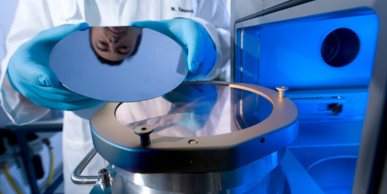
The German research institute is working to develop advanced, high-resolution material and thin-film characterization methods that could evolve into a range of simplified and rapid measurement procedures for routine use in intellectual property research.
The German Fraunhofer Center for Silicon Photovoltaics (Fraunhofer CSP) is developing a range of high-resolution material and thin-film microscopic and nanoscopic characterization methods for use in the analysis of patent infringements on higher efficiency solar PV products.
The work is part of a project known in Germany as IP-Schutz. The project, which will run until March 2027, will provide researchers with the necessary framework to develop experimental techniques as a basis for reliable intellectual property (IP) and patent infringement investigation services for project partners and customers.
The expected outcome is a set of simplified and rapid measurement procedures for routine use in IP investigations, enabling legally secure evidence.
The effort is driven by the increasing number of patent lawsuits pending in many regions around the world, said Stefan Lange, team manager and IP-Schutz project leader at Fraunhofer CSP.
“Today, cost-efficient and highly automated production of PV cells and modules can be achieved almost anywhere, but the development of new solar cell and module technologies is time-consuming and expensive,” said Lange. pv magazine. “Often, patents only cover microscopic or nanoscopic features or thin-film interfaces whose properties are difficult to characterize.”
PV technologies such as tunnel oxide passivated contact (TOPCon), silicon heterojunction (SHJ) and interdigitated back contact (IBC) devices require more advanced analysis methods with greater spatial resolution and measurement sensitivity, according to Lange.
Some of the relevant non-destructive measurement technologies and large area preparation methods that Fraunhofer CSP will use are plasma polishing and pulsed laser ablation, as well as time of flight SIMS (ToF-SIMS), transmission electron microscopy (TEM) and X-ray. photoelectron spectroscopy (XPS) to investigate cell interfaces, microscopic current paths and passivation layers.
Lange pointed out that this type of research differs from conventional research and development (R&D) because the methods must be adapted to the commercial module samples, not the other way around.
“At Fraunhofer CSP we already have significant experience in R&D services such as analyzing cells from commercial modules, writing technical reports and expert opinions, all with legal security,” he said, adding that the documentation is more extensive and thorough than typical R&D support. and there is no room for error.
Together with research partner Anhalt University of Applied Sciences, the Fraunhofer CSP has already collected information and material samples from industrial partners to understand their patent-related needs.
This content is copyrighted and may not be reused. If you would like to collaborate with us and reuse some of our content, please contact: editors@pv-magazine.com.
Popular content


