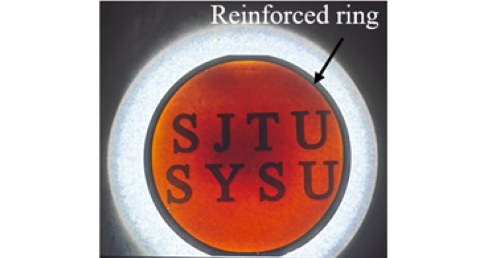
A research team in China has developed a new thin silicon wafer reinforced ring (TSRR) to protect ultra-thin wafers and solar cells during production. This technique consists of applying the ring to the edge of thin wafers and is compatible with all silicon solar panel technology.
A research team from China’s Shanghai Jiao Tong University and Sun Yat-sen University has shown that applying a new thin silicon wafer reinforced ring (TSRR) to the edge of thin wafers makes the PV material much less susceptible to breakage. The TSRR was demonstrated on silicon wafers with a thickness of 4.7 μm, solar cells with a thickness of 28 μm and larger wafers with a thickness of 60 μm.
“Our team has developed a new technique compatible with industrial manufacturing processes to enable the use of ultra-thin crystalline silicon wafers that are smaller than 60 μm and can be as thin as 20 μm. The technology makes the cells radically less brittle,” says researcher Taojian Wu pv magazine.
“We were surprised that there was a 4-in [100 mm] wafer with a thickness of less than 5 µm could be obtained by a simple reinforced ring method, and that with this method we can easily make 28 µm silicon solar cells with an efficiency of more than 20%,” said Wu, adding that subtle improvements in the ‘structure of thin silicon’ has led to such ‘great progress’.
In the study, the team first constructed a free-standing 4.7 μm-thick 4-inch (100mm) wafer with TSRR. It then used TSRR to create doping-free 28 μm silicon cells with interdigitated back contacts (IBC), resulting in a breakage rate of approximately 0%. The cell efficiency achieved was 20.33% and was certified at 20.05%.
This was the highest efficiency reported for silicon solar cells with a thickness of less than 35 μm, according to more than a decade of performance data in the literature collected by the team.
The researchers noted that the TSRR method requires only three more production steps than conventional PV mass production. It first deposits a 70 nm layer of silicon nitride (SiNx) on both sides of conventionally thick silicon wafers by plasma-enhanced chemical vapor deposition (PECVD) or low-pressure chemical vapor deposition (LPCVD), after which the SiNx is removed from the central region. of one side using a die, laser or photolithography, to create an opening, and followed by an etching step with an alkaline solution to the desired thickness, the team said.
The SiNx layer provides protection and ensures that the silicon in the edge area of the wafer retains its original thickness, the research team explains. “The difficult part is the process of applying a high-quality SiNx protective film, which must be able to withstand long-term etching with an alkaline solution,” said Wu. “The easy part is the manufacturing process of thin silicon solar cells, because we can process thin silicon wafers with reinforced rings in the same way as normal silicon wafers.”
The team claimed that the TSRR structure is applicable to “any silicon technology,” such as passivated emitter and back cell (PERC), silicon heterojunction (SHJ), tunnel oxide passivating contact (TOPCon), as well as doping-free passivating contact xBC cell technologies.
To better understand the optoelectric performance of the experimental solar cells, the team performed a numerical TCAD simulation of solar cells with front and back contacts (FBC). The experiments and mechanical property simulations comparing TSRR with conventional thin silicon structures confirmed the supporting role of the TSRR, the research group said.
The team also prepared textured TSRR wafers from 50 μm to 60 μm, with dimensions of 182 mm x 182 mm, and performed key manufacturing processes to confirm the industrial compatibility of the TSRR method. “We have received feedback from our partner company that the breakage rate during the manufacturing of 60 μm-SHJ solar cells has been significantly reduced,” said Wu.
The research is described in detail in “Free-standing ultra-thin silicon wafers and solar cells through edge reinforcement,” published by communication about nature.
This content is copyrighted and may not be reused. If you would like to collaborate with us and reuse some of our content, please contact: editors@pv-magazine.com.


