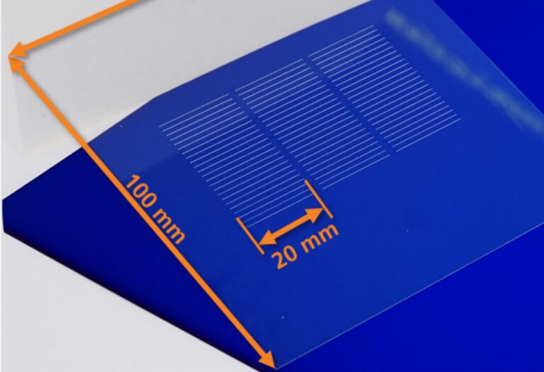
Fraunhofer ISE researchers have developed a new metallization process that can produce ultra-fine line contacts for solar cells. The proposed technique is based on the so-called LIDE technology and can reportedly help increase the overall efficiency of PV devices.
A team of researchers from Germany’s Fraunhofer Institute for Solar Energy Systems (Fraunhofer ISE) and German technology company LPKF Laser & Electronics SE have developed a low-temperature metallization process to print ultra-fine metal contact fingers used in solar cells.
Narrower ultra-fine line contacts can reduce the shadow on the front of solar cells, improving their overall efficiency and performance.
“The industry trend is towards increasingly narrower fingers, with the aim of reaching a finger width of 15 μm by 2034, as highlighted in the ITRPV 2024 report,” the research group explains. “This drive for reduction is not only driven by efficiency gains, but also by the reduced use of precious silver (Ag) in the production of solar cells.”
In the study “Advanced fine line printing with glass stencils: reaching metal contact fingers under 10 μm”, published in Progress in photovoltaicsthe scientists explained that the solar industry has managed to reduce the finger width from 120 μm in 2005 to less than 20 μm in 2024.
The proposed metallization process is based on glass stencils supplied by LPKF Laser & Electronics SE. These stencils depend on the so-called LIDE technology, a two-step process that creates deep structures in thin glass with a high aspect ratio in the range of more than 1:10 at a high processing speed. “This process is not only fast but also cost-efficient, allowing the production of point or line-shaped structures down to 5 μm and less,” the academics pointed out.
They also explained that they used the LIDE technique to initially modify a 400 μm thick sheet of 10 cm x 10 cm AF 32 eco-glass. They then used wet chemical etching to remove the laser-modified glass faster than the unmodified areas, which they say resulted in highly accurate microstructures. Additionally, they used a laser process to structure the glass for the opening of the final opening channel on the other side of the window film.
Using complex cross-sectional geometries of the print channels in the glass film, the academics were able to create 290 μm stencils with mask opening widths of 10 μm, 7.5 μm and up to 5 μm, allowing them to fabricate line contacts with core widths of approximately 8.4 μm and nominal opening widths of 7.5 μm and 10 μm respectively.
The group explained that this low finger height resulted in metal contacts with aspect ratios of approximately 0.19. Aspect ratio defines the ratio between the width and height of an image or screen.
“Reducing the length of the orifice channel in the glass stencils from 50 μm to 25 μm and using thinner glass films increased the finger height, resulting in aspect ratios of 0.35,” it further explained. “The aspect ratio was further improved to 0.45 by using a nanoparticle-based Ag paste at low temperature, which also improved the homogeneity of the fingers compared to a microparticle-based Ag paste.”
Looking ahead, the scientists said they want to implement the new process via a screen printer, which could improve printing results through quantitative optimization. “In addition, quantifiable results in electrical performance and IV measurements on solar cells will be obtained, demonstrating the optoelectronic benefits of stencil-printed contacts,” they concluded.
This content is copyrighted and may not be reused. If you would like to collaborate with us and reuse some of our content, please contact: editors@pv-magazine.com.


