Scientists in the Netherlands have proposed a new test scheme for recycling silicon from photovoltaic panels at the end of their life. Their methodology helped create several wafer categories for recycling silicon for the production of new ingots, but also showed that most of the recycled silicon in the near future will come from p-type products, which will hardly be reused in a market now dominated by n-type modules.
A research group coordinated by the Netherlands Organization for Applied Scientific Research (TNO) has investigated how cleaned wafers or wafer fragments recovered from end-of-life (EoL) PV modules can be reused for the production of new crystalline silicon ingots and found that gallium-doped wafers could be particularly suitable for this purpose.
The scientists explained that silicon must be removed from the discarded wafers by eliminating any contamination on the surfaces, which would reinstate it in the category of high-purity materials. “The main pollutants are dopants, oxygen, carbon and perhaps some nitrogen,” says the study’s lead author. Bart Geerligs, told pv magazine. “We looked at this mainly from the perspective of doping and resistance control, and to a limited extent also from the perspective of other residual contaminants.”
In the study “Potential for recycled silicon solar cells as raw material for the growth of new blocks”, published in Progress in photovoltaicsthe researchers explained that their analysis concerned potential technical and economic limitations mainly related to dopants and impurities. They also expect that significant amounts of silicon can be recovered by around 2040, especially from p-type wafers, and that the markets for boron and gallium doping will be more or less equally divided.
The research group also created a methodology to separate n-type and p-type modules, and boron-doped versus boron-doped or gallium-doped p-type panels. For example, it was found that if the solar cells in the module are polycrystalline, they are necessarily p-type B doped. “To our knowledge, there has been no commercial production of n-type modules based on polycrystalline silicon,” the academics said.
Furthermore, they created a separation between wafers that may or may not have metallization on the front. They also said that voltage must be identified for all modules except those based on interdigitated back-contact (IBC) cell technology, and a visual inspection must be performed on the back of all cells. “The principle for the inspection then is that all industrial p-type Al-BSF and PERC cells have Al backside metallization combined with local silver pads for soldering the interconnected ribbons, and industrial n-type cells have no such. combination,” they specified.
The team explained that the entire test scheme can be bypassed if a label on the discarded panel contains useful information. “For example, a module may be documented to contain HJT (n-type) cells or may be based on IBC cells from a manufacturer such as Sunpower or Maxeon,” it further explains. “It would also be very helpful if PERC modules visibly show a production date, as this would imply board doping before 2019, and after 2022 it would imply gallium doping of the wafers.”
“This arrangement would result in three material flows,” Geerligs said. “These are n-type doped cells, p-type boron doped cells and a stream of monocrystalline PERC cells that can be either boron or gallium doped.”
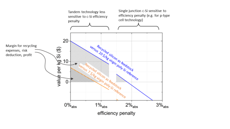
The scientists concluded that reusing p-type wafers as raw material for new p-type blocks will not be economically feasible, as n-type cells are now the dominant technology.
“The potential cost savings from using recycled raw materials does not appear to be sufficient to compensate for this,” they say. “Another opportunity for much better profitability for recycling p-type wafers may become available with perovskite-silicon tandem technology, in which case both the efficiency disadvantage over n-type is greatly reduced and PERC cell performance can be improved. enhanced by a poly – Si transmitter.”
This content is copyrighted and may not be reused. If you would like to collaborate with us and reuse some of our content, please contact: editors@pv-magazine.com.


